
Sony has succeeded in developing the world’s first stacked CMOS image sensor technology with 2-Layer Transistor Pixel.
While conventional CMOS image sensors’ photodiodes and pixel transistors occupy the same substrate, Sony’s new technology separates photodiodes and pixel transistors on different substrate layers. This new architecture doubles saturation signal level relative to conventional image sensors widens dynamic range and reduces noise. What is more, the new technology’s pixel structure enables pixels to maintain or improve their existing properties at not only current but also smaller pixel sizes.
Sony announced this breakthrough at this year’s IEEE International Electron Devices Meeting.
A stacked CMOS image sensor uses a stacked structure consisting of a pixel chip made up of back-illuminated pixels stacked atop a logic chip where signal processing circuits are formed. The pixel chip, photodiodes for converting light to electrical signals, and pixel transistors for controlling the signals are situated alongside each other on the same layer. By increasing saturation signal level within form-factor constraints, the image quality realizes with a wide dynamic range.
Sony’s new architecture is an advancement in stacked CMOS image sensor technology of packaged photodiodes and pixel transistors on separate substrates stacked one atop the other.
In conventional stacked CMOS image sensors, by contrast, the photodiodes and pixel transistors sit alongside each other on the same substrate. The new stacking technology enables the adoption of architectures that allow the photodiode and pixel transistor layers to be optimized. This doubles saturation signal level relative to conventional image sensors and widens the dynamic range.
What is more, by increasing the amp transistor size, Sony succeeded in substantially reducing the noise to which nighttime and other dark-location images are prone. The widened dynamic range and noise reduction available from this new technology will prevent underexposure and overexposure in settings with a combination of bright and dim illumination.
Sony will contribute to the realization of increasingly high-quality imaging such as smartphone photographs with its 2-Layer Transistor Pixel technology.
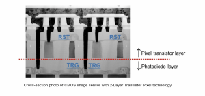
Photo Credits: Sony